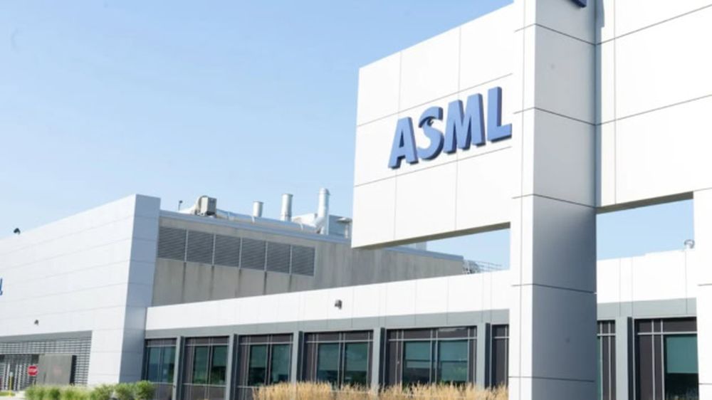
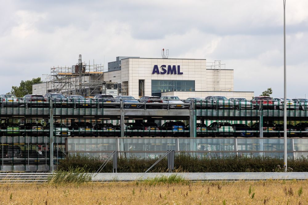
ASML has broken ground on what looks, at first glance, like another enormous industrial expansion. But the scale of the project raises a much more interesting question: what does ASML know about the future of computing that makes such an investment necessary? Its new BIC North campus near Eindhoven is planned across roughly 35 hectares and could eventually accommodate as many as 20,000 people. The first phase is expected to include offices, logistics facilities and advanced manufacturing space, with completion targeted for 2029. This is not simply a company adding a few production lines. It looks more like an industrial bet on a semiconductor market that is preparing for another transformation.
The obvious suspect is artificial intelligence. The spectacular growth of AI has created an almost insatiable demand for increasingly powerful processors, and behind every generation of advanced AI hardware sits an extraordinary manufacturing problem. The computational power required by modern models is pushing chipmakers toward larger, denser and more sophisticated designs, while the number of chips required by hyperscale data centers continues to explode. ASML occupies a particularly unusual position in this chain because its extreme ultraviolet lithography technology is essential for producing the most advanced semiconductor features. In other words, when chipmakers want to manufacture tomorrow’s processors, they increasingly need machines that only ASML can provide.
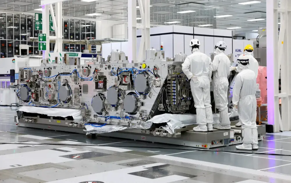
That makes ASML’s next move even more revealing. Its High-NA EUV technology is already entering the next generation of semiconductor manufacturing, promising finer patterning and potentially more powerful chips. Yet the industry is encountering another limitation: how large a chip can actually be manufactured efficiently. AI accelerators are becoming enormous, and conventional approaches increasingly force designers to divide computational workloads across multiple chips or complex packages. ASML is therefore investigating ways to use larger masks with High-NA systems, potentially allowing substantially larger dies to be manufactured. If that succeeds, lithography itself could become one of the technologies determining how far the current AI scaling race can continue.
There is therefore a bigger story behind the concrete being poured in Eindhoven. ASML is effectively expanding the machinery behind the machinery of the AI revolution. TSMC, Samsung, Intel and other manufacturers can spend billions building new fabs, but those factories cannot produce the most advanced chips without the extraordinarily complex lithography equipment required to pattern them. The bottleneck is moving upstream, and ASML is positioning itself accordingly. The enormous new campus may consequently be less a response to today’s semiconductor demand than a preparation for an industry in which AI requires vastly more computing power, vastly more advanced chips and, ultimately, vastly more machines capable of making them. The real question is no longer whether AI will consume more chips. It is whether the semiconductor industry can build the infrastructure fast enough to satisfy what AI is becoming.

#ASML #EUV #HighNAEUV #ArtificialIntelligence #AIChips #Semiconductors #TSMC #Nvidia #ChipManufacturing #Technology